
Potenza mosfet smd 110v STC2326
Ottieni l'ultimo prezzo| Tipo di pagamento: | L/C,T/T,Paypal |
| Incoterm: | FOB,CFR,CIF |
| Trasporti: | Ocean,Air |
| Porta: | SHANGHAI |

| Tipo di pagamento: | L/C,T/T,Paypal |
| Incoterm: | FOB,CFR,CIF |
| Trasporti: | Ocean,Air |
| Porta: | SHANGHAI |
Modello: YZPST-STC2326
marchio: YZPST
B Triac serie TA30
YZPST-STC2326
DESCRIZIONE
L'STC2326 è il transistor a effetto di campo di potenza in modalità di ottimizzazione logica N-Channel prodotto con tecnologia DMOS ad altissima densità cellulare. L'STC2326 è stato progettato specificamente per migliorare l'efficienza complessiva dei convertitori CC / CC utilizzando i controller PWM di commutazione sincroni o convenzionali. È stato ottimizzato per la bassa carica del gate, basso RDS (ON) e velocità di commutazione rapida.
APPLICAZIONI
Sistema alimentato
Convertitore DC / DC
Interruttore di carico
CARATTERISTICHE
110V / 3A, RDS (ON) = 310mΩ @ VGS = 10V
Design a celle ad alta densità per RDS estremamente basso (ON)
Eccezionale resistenza alla corrente e massima corrente continua
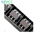
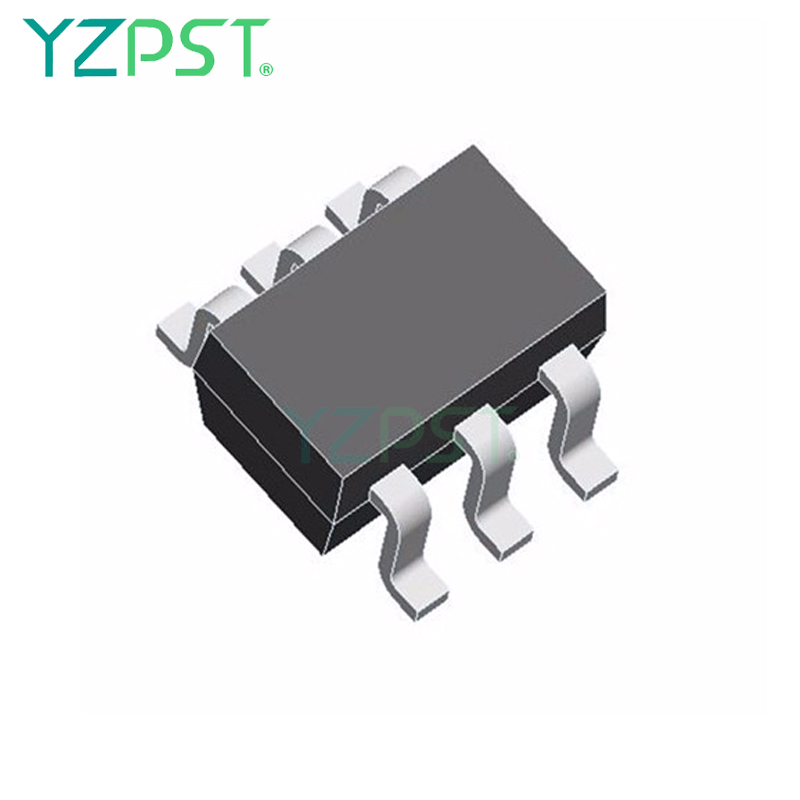
Design della confezione SOT-23-6L
CONFIGURAZIONE PIN (SOT-23-6L)
")
|
Pin |
Symbol |
Description |
|
1 |
D |
Drain |
|
2 |
D |
Drain |
|
3 |
G |
Gate |
|
4 |
S |
Source |
|
5 |
D |
Drain |
|
6 |
D |
Drain |
O RDER ING IN F O R M A T I O N
|
Part Number |
Package |
Part Marking |
|
SPN2326S26RGB |
SOT-23-6L |
26YW |
A B SOU L T E MA X I M U M R A T IN G S ( T A = 25 ℃ U n l e s s O T E R w i s e n o t d )
|
Parameter |
Symbol |
Typical |
Unit |
|
|
Drain-Source Voltage |
VDSS |
110 |
V |
|
|
Gate –Source Voltage |
VGSS |
±20 |
V |
|
|
Continuous Drain Current(TJ=150℃) |
TA=25℃ |
ID |
3.0 |
A |
|
TA=70℃ |
2.0 |
|||
|
Pulsed Drain Current |
IDM |
10 |
A |
|
|
Power Dissipation |
TA=25℃ |
PD |
2.0 |
W |
|
TA=70℃ |
1.3 |
|||
|
Operating Junction Temperature |
TJ |
-55/150 |
℃ |
|
|
Storage Temperature Range |
TSTG |
-55/150 |
℃ |
|
|
Thermal Resistance-Junction to Ambient |
RθJA |
62.5 |
℃/W |
|
|
Parameter |
Symbol |
Conditions |
Min. |
Typ |
Max. |
Unit |
|
Static |
||||||
|
Drain-Source Breakdown Voltage |
V(BR)DSS |
VGS=0V,ID=250uA |
110 |
|
|
V |
|
Gate Threshold Voltage |
VGS(th) |
VDS=VGS,ID=250uA |
1 |
2.0 |
2.5 |
|
|
Gate Leakage Current |
IGSS |
VDS=0V,VGS=±20V |
|
|
±100 |
nA |
|
Zero Gate Voltage Drain Current |
IDSS |
VDS=80V,VGS=0V |
|
|
1 |
uA |
|
VDS=80V,VGS=0V TJ=125℃ |
|
|
5 |
|||
|
On-State Drain Current |
ID(on) |
VDS≥5V,VGS =10V |
3.0 |
|
|
A |
|
Drain-Source On-Resistance |
RDS(on) |
VGS= 10V,ID=3A |
|
0.26 |
0.31 |
Ω |
|
Forward Transconductance |
gfs |
VDS=10V,ID=3A |
|
2.4 |
|
S |
|
Diode Forward Voltage |
VSD |
IS=1A,VGS =0V |
|
|
1.2 |
V |
|
Dynamic |
||||||
|
Total Gate Charge |
Qg |
VDS=80V,VGS=10V ID= 5A |
|
9 |
13 |
nC |
|
Gate-Source Charge |
Qgs |
|
2 |
|
||
|
Gate-Drain Charge |
Qgd |
|
1.4 |
|
||
|
Input Capacitance |
Ciss |
VDS=25,VGS=0V f=1MHz |
|
508 |
|
pF |
|
Output Capacitance |
Coss |
|
29 |
|
||
|
Reverse Transfer Capacitance |
Crss |
|
16.5 |
|
||
|
Turn-On Time |
td(on) |
VDD=50V,RL=10Ω ID=3A,VGEN=10V RG=3.3Ω |
|
2 |
|
nS |
|
tr |
|
21.5 |
|
|||
|
Turn-Off Time |
td(off) |
|
11.2 |
|
||
|
tf |
|
18.8 |
|
|||
")
")


Numero Di Telefono: 86-514-87782298
Whatsapp: +8613805278321
Azienda Indirizzo: 3rd Floor, Weiheng Building No.20 B Area, Yangzhou, Jiangsu China
sito web: https://it.yzpst.com


Privacy statement: Your privacy is very important to Us. Our company promises not to disclose your personal information to any external company with out your explicit permission.
Fill in more information so that we can get in touch with you faster
Privacy statement: Your privacy is very important to Us. Our company promises not to disclose your personal information to any external company with out your explicit permission.