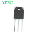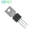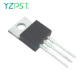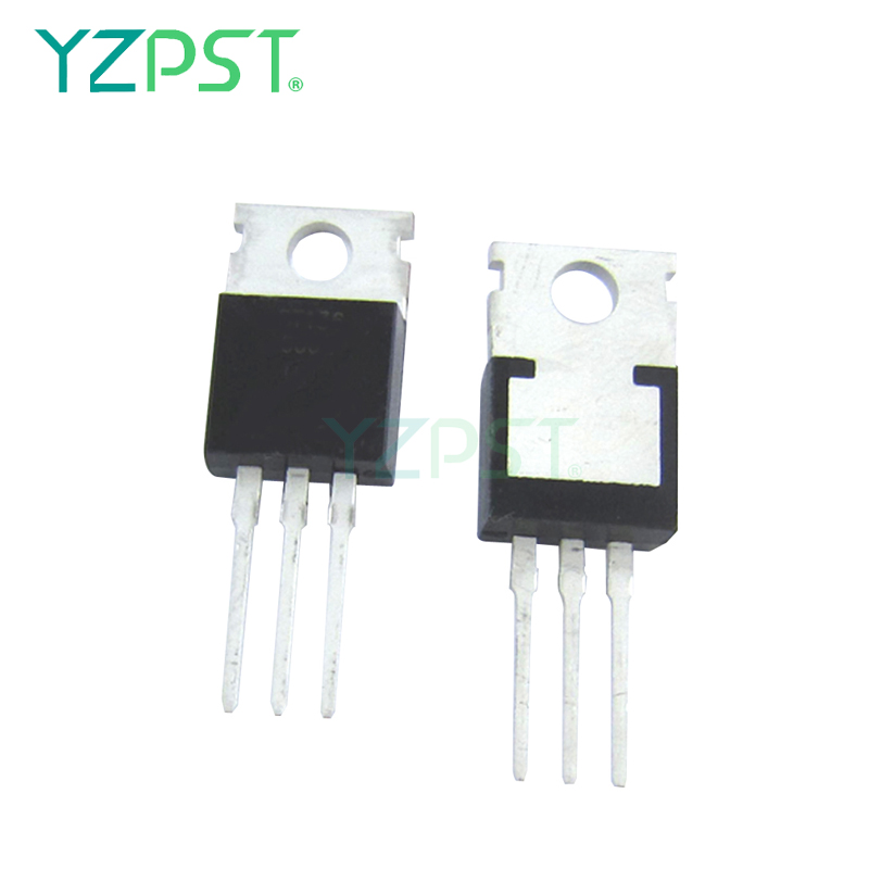
TO-220 controllo di fase scr 25A Transistor 25TTS12
$0.252000-99999 Piece/Pieces
$0.22≥100000Piece/Pieces
| Tipo di pagamento: | L/C,T/T,Paypal |
| Incoterm: | FOB,CFR,CIF |
| Quantità di ordine minimo: | 2000 Piece/Pieces |
| Trasporti: | Ocean,Air |
| Porta: | SHANGHAI |

$0.252000-99999 Piece/Pieces
$0.22≥100000Piece/Pieces
| Tipo di pagamento: | L/C,T/T,Paypal |
| Incoterm: | FOB,CFR,CIF |
| Quantità di ordine minimo: | 2000 Piece/Pieces |
| Trasporti: | Ocean,Air |
| Porta: | SHANGHAI |
Modello: YZPST-25TTS12
marchio: YZPST
| Unità vendibili | : | Piece/Pieces |
| Tipo pacchetto | : | 1. Imballaggio anti-elettrostatico 2. Scatola di cartone 3. Imballaggio protettivo in plastica |
Phase Control SCR, 25 A
DESCRIZIONE / CARATTERISTICHE
I 25TTS ... High Voltage Series di raddrizzatori controllati al silicio sono progettati specificamente per applicazioni di commutazione di potenza e controllo di fase di media potenza. La tecnologia di passivazione del vetro utilizzata ha un funzionamento affidabile fino a
125 ° C temperatura di giunzione.
Le applicazioni tipiche sono in rettifica di input (avvio graduale) e questi prodotti sono progettati per essere utilizzati con diodi di ingresso Vishay HPP, interruttori e raddrizzatori di uscita disponibili in identici contorni del pacchetto.
Questo prodotto è stato progettato e qualificato per il livello industriale.

|
PRODUCT SUMMARY |
|
|
VT at 16 A |
< 1.25 V |
|
ITSM |
300 A |
|
VRRM |
800/1200 V |
|
OUTPUT CURRENT IN TYPICAL APPLICATIONS |
|||
|
APPLICATIONS |
SINGLE-PHASE BRIDGE |
THREE-PHASE BRIDGE |
UNITS |
|
Capacitive input filter TA = 55 °C, TJ = 125 °C, common heatsink of 1 °C/W |
18 |
22 |
A |
|
MAJOR RATINGS AND CHARACTERISTICS |
|||
|
PARAMETER |
TEST CONDITIONS |
VALUES |
UNITS |
|
IT(AV) |
Sinusoidal waveform |
16 |
A |
|
IRMS |
|
25 |
|
|
VRRM/VDRM |
|
800/1200 |
V |
|
ITSM |
|
300 |
A |
|
VT |
16 A, TJ = 25 °C |
1.25 |
V |
|
dV/dt |
|
500 |
V/µs |
|
dI/dt |
|
150 |
A/µs |
|
TJ |
|
- 40 to 125 |
°C |
|
VOLTAGE RATINGS |
|||
|
PART NUMBER |
VRRM, MAXIMUM PEAK REVERSE VOLTAGE V |
VDRM, MAXIMUM PEAK DIRECT VOLTAGE V |
IRRM/IDRM AT 125 °C mA |
|
25TTS08 |
800 |
800 |
10 |
|
25TTS12 |
1200 |
1200 |
|
|
ABSOLUTE MAXIMUM RATINGS |
||||||
|
PARAMETER |
SYMBOL |
TEST CONDITIONS |
VALUES |
UNITS |
||
|
TYP. |
MAX. |
|||||
|
Maximum average on-state current |
IT(AV) |
TC = 93 °C, 180° conduction half sine wave |
16 |
A |
||
|
Maximum RMS on-state current |
IRMS |
|
25 |
|||
|
Maximum peak, one-cycle, non-repetitive surge current |
ITSM |
10 ms sine pulse, rated VRRM applied |
300 |
|||
|
10 ms sine pulse, no voltage reapplied |
350 |
|||||
|
Maximum I2t for fusing |
I2t |
10 ms sine pulse, rated VRRM applied |
450 |
A2s |
||
|
10 ms sine pulse, no voltage reapplied |
630 |
|||||
|
Maximum I2√t for fusing |
I2√t |
t = 0.1 to 10 ms, no voltage reapplied |
6300 |
A2√s |
||
|
Maximum on-state voltage drop |
VTM |
16 A, TJ = 25 °C |
1.25 |
V |
||
|
On-state slope resistance |
rt |
TJ = 125 °C |
12.0 |
mΩ |
||
|
Threshold voltage |
VT(TO) |
1.0 |
V |
|||
|
Maximum reverse and direct leakage current |
IRM/IDM |
TJ = 25 °C |
VR = Rated VRRM/VDRM |
0.5 |
mA |
|
|
TJ = 125 °C |
10 |
|||||
|
Holding current |
IH |
Anode supply = 6 V, resistive load, initial IT = 1 A |
- |
100 |
||
|
Maximum latching current |
IL |
Anode supply = 6 V, resistive load |
200 |
|||
|
Maximum rate of rise of off-state voltage |
dV/dt |
|
500 |
V/µs |
||
|
Maximum rate of rise of turned-on current |
dI/dt |
|
150 |
A/µs |
||
|
TRIGGERING |
||||
|
PARAMETER |
SYMBOL |
TEST CONDITIONS |
VALUES |
UNITS |
|
Maximum peak gate power |
PGM |
|
8.0 |
W |
|
Maximum average gate power |
PG(AV) |
|
2.0 |
|
|
Maximum peak positive gate current |
+ IGM |
|
1.5 |
A |
|
Maximum peak negative gate voltage |
- VGM |
|
10 |
V |
|
Maximum required DC gate current to trigger |
IGT |
Anode supply = 6 V, resistive load, TJ = - 10 °C |
60 |
mA |
|
Anode supply = 6 V, resistive load, TJ = 25 °C |
45 |
|||
|
Anode supply = 6 V, resistive load, TJ = 125 °C |
20 |
|||
|
Maximum required DC gate voltage to trigger |
VGT |
Anode supply = 6 V, resistive load, TJ = - 10 °C |
2.5 |
V |
|
Anode supply = 6 V, resistive load, TJ = 25 °C |
2.0 |
|||
|
Anode supply = 6 V, resistive load, TJ = 125 °C |
1.0 |
|||
|
Maximum DC gate voltage not to trigger |
VGD |
TJ = 125 °C, VDRM = Rated value |
0.25 |
|
|
Maximum DC gate current not to trigger |
IGD |
2.0 |
mA |
|
|
SWITCHING |
||||
|
PARAMETER |
SYMBOL |
TEST CONDITIONS |
VALUES |
UNITS |
|
Typical turn-on time |
tgt |
TJ = 25 °C |
0.9 |
µs |
|
Typical reverse recovery time |
trr |
TJ = 125 °C |
4 |
|
|
Typical turn-off time |
tq |
110 |
||
|
THERMAL AND MECHANICAL SPECIFICATIONS |
|||||
|
PARAMETER |
SYMBOL |
TEST CONDITIONS |
VALUES |
UNITS |
|
|
Maximum junction and storage temperature range |
TJ, TStg |
|
- 40 to 125 |
°C |
|
|
Maximum thermal resistance, junction to case |
RthJC |
DC operation |
1.1 |
°C/W |
|
|
Maximum thermal resistance, junction to ambient |
RthJA |
|
62 |
||
|
Typical thermal resistance, case to heatsink |
RthCS |
Mounting surface, smooth and greased |
0.5 |
||
|
Approximate weight |
|
|
2 |
g |
|
|
0.07 |
oz. |
||||
|
Mounting torque |
minimum |
|
|
6 (5) |
kgf · cm (lbf · in) |
|
maximum |
|
|
12 (10) |
||
|
Marking device |
|
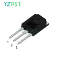
Case style TO-220AB |
25TTS08 |
||
|
25TTS12 |
|||||


Numero Di Telefono: 86-514-87782298
Whatsapp: +8613805278321
Azienda Indirizzo: 3rd Floor, Weiheng Building No.20 B Area, Yangzhou, Jiangsu China
sito web: https://it.yzpst.com


Privacy statement: Your privacy is very important to Us. Our company promises not to disclose your personal information to any external company with out your explicit permission.
Fill in more information so that we can get in touch with you faster
Privacy statement: Your privacy is very important to Us. Our company promises not to disclose your personal information to any external company with out your explicit permission.